Interconnects: PCIe, CXL, NVLink, and the Emerging Composable-Disaggregated Architecture
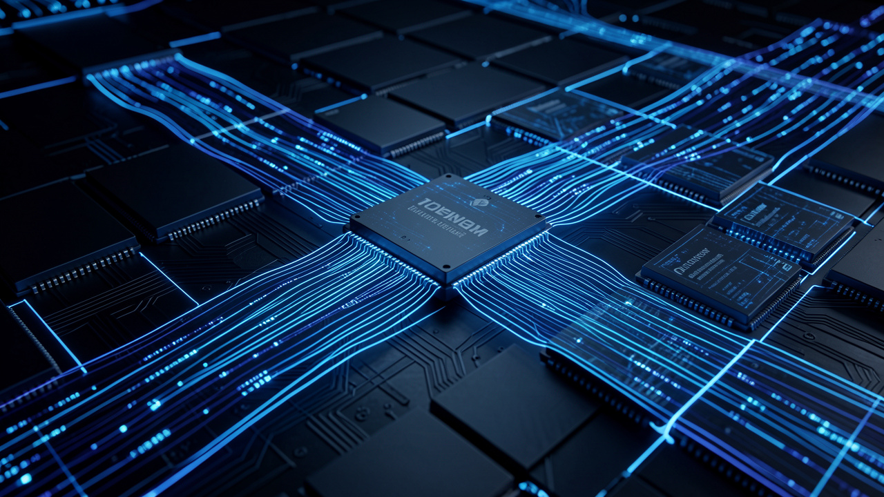
A deep technical survey of modern interconnects—PCIe generations 1-6, CXL.io/cache/memory protocols, NVLink and NVSwitch—and how they enable composable-disaggregated infrastructure.
Contents
The dominant architecture for servers has been the monolithic motherboard: CPU, memory, storage, and networking all soldered or socketed onto a single board, connected by fixed-width buses. This architecture is simple but inflexible. If a workload needs more memory bandwidth than the CPU’s memory controllers provide, you must replace the entire server. If a workload needs GPU acceleration, you add a PCIe card—limited by the PCIe slot’s bandwidth and the physical space inside the chassis. The ratio of CPU cores to memory capacity to accelerator count is fixed at purchase time and cannot be adjusted to match changing workload demands.
The composable-disaggregated infrastructure (CDI) vision, championed by Intel’s CXL (Compute Express Link) and NVIDIA’s NVLink/NVSwitch, proposes a radical alternative: disaggregate the CPU, memory, accelerators, and storage into independent resource pools connected by a high-speed, low-latency, cache-coherent interconnect. Compose a “server” on the fly by allocating resources from these pools, matching the specific needs of each workload. When the workload changes, recompose the server without physically touching hardware.
This vision is technically audacious and commercially consequential. It would transform the data center from a collection of static servers into a fluid, programmable resource fabric. It requires interconnects that are an order of magnitude faster and lower-latency than current PCIe, with cache coherence across the fabric, and with the reliability to maintain memory semantics over distances of meters (across a rack). This article surveys the interconnect landscape: PCIe (the incumbent), CXL (the disruptor), and NVLink (the GPU-optimized alternative), examining their protocols, their performance, and their roles in the emerging disaggregated architecture.
1. PCIe: The Universal Interconnect
Peripheral Component Interconnect Express (PCIe) is the dominant I/O interconnect for virtually all modern computers. It connects CPUs to GPUs, NVMe SSDs, network interface cards, and a vast ecosystem of peripherals. PCIe has evolved through six generations, each doubling the per-lane bandwidth:
| Generation | Year | Per-lane bandwidth | x16 bandwidth (bidirectional) | Signaling |
|---|---|---|---|---|
| PCIe 1.0 | 2003 | 2.5 GT/s (250 MB/s) | 8 GB/s | 2.5 GHz, 8b/10b |
| PCIe 2.0 | 2007 | 5 GT/s (500 MB/s) | 16 GB/s | 5 GHz, 8b/10b |
| PCIe 3.0 | 2010 | 8 GT/s (~1 GB/s) | 32 GB/s | 8 GHz, 128b/130b |
| PCIe 4.0 | 2017 | 16 GT/s (~2 GB/s) | 64 GB/s | 16 GHz, 128b/130b |
| PCIe 5.0 | 2019 | 32 GT/s (~4 GB/s) | 128 GB/s | 32 GHz, 128b/130b |
| PCIe 6.0 | 2022 | 64 GT/s (~8 GB/s) | 256 GB/s | 32 GHz, PAM4, FEC |
PCIe 6.0 introduces two fundamental changes: PAM4 signaling (pulse amplitude modulation with 4 levels, encoding 2 bits per symbol instead of NRZ’s 1 bit per symbol) and forward error correction (FEC) to compensate for the higher bit error rate of PAM4. These changes allow PCIe 6.0 to double the bandwidth without doubling the clock frequency (which would be infeasible due to signal integrity constraints on copper traces). The tradeoff is increased latency (FEC adds ~2 ns of processing delay) and increased power per bit.
PCIe uses a tree topology: a root complex (integrated into the CPU) connects to endpoints (devices) and switches (which fan out to more endpoints). The tree is non-coherent: the CPU does not automatically snoop device memory, and devices must use explicit DMA to access host memory. This non-coherence is the fundamental limitation that CXL addresses.
2. CXL: Cache-Coherent Interconnect for Disaggregation
Compute Express Link (CXL), introduced in 2019 and standardized by the CXL Consortium (Intel, AMD, ARM, and dozens of industry partners), is built on top of the PCIe physical layer (PCIe 5.0 for CXL 1.1/2.0, PCIe 6.0 for CXL 3.0) but adds three new protocols above the physical layer:
CXL.io: Essentially PCIe’s I/O protocol (TLP, DMA, MSI-X interrupts). Used for device discovery, configuration, and non-coherent data transfer. This is the baseline that every CXL device must support.
CXL.cache: Allows a CXL device (typically an accelerator with its own cache) to cache host memory coherently. The device issues snoop requests to the host CPU’s cache hierarchy, and the host can snoop the device’s cache. This is the “Type 2” CXL device model (devices with caches, like GPUs and FPGAs with coherent access to host memory).
CXL.memory (CXL.mem): Allows the host CPU to access device-attached memory with load/store semantics (byte-addressable, not block-addressable like NVMe). This is the “Type 3” CXL device model (memory expanders and persistent memory devices). The host CPU maps the device’s memory into its physical address space and accesses it with regular loads and stores, cached in the CPU’s cache hierarchy.
CXL enables three transformative use cases:
Memory expansion (Type 3): Attach CXL memory modules (DDR5 on a CXL controller, or storage-class memory) to increase memory capacity beyond the CPU’s native DRAM slots, without adding CPU sockets. This is the first CXL use case to reach production (Intel Sapphire Rapids with CXL 1.1, 2023; AMD EPYC Genoa with CXL 1.1, 2023).
Memory pooling: Multiple CPUs share a pool of CXL-attached memory, dynamically allocating capacity to whichever CPU needs it. This enables memory oversubscription (allocating more memory to VMs than physically exists, relying on the fact that not all VMs use their full allocation simultaneously) and reduces stranded memory (memory installed in an underutilized server that cannot be used by a neighboring server).
Accelerator coherency (Type 2): GPUs, FPGAs, and AI accelerators access host memory coherently, eliminating the need for explicit DMA and enabling fine-grained sharing of data structures between CPU and accelerator. This is the “holy grail” of heterogeneous computing, and CXL 3.0 (2024) adds the multi-level switching and memory sharing features needed to make it practical.
2.1 CXL 3.0: Fabric Capabilities
CXL 3.0 (2024) transforms CXL from a point-to-point interconnect into a fabric: multiple hosts and multiple devices can be connected through CXL switches, with coherent memory sharing across the entire fabric. Key new features:
- Multi-head devices: A single CXL device can be simultaneously connected to multiple hosts, with each host accessing a partitioned portion of the device’s memory.
- Global fabric-attached memory (GFAM): Memory in the CXL fabric is shared among all hosts, with hardware-enforced coherence (using the CXL 3.0 coherence protocol, based on a distributed directory).
- Peer-to-peer DMA: Devices can directly transfer data to each other without involving the host CPU, reducing latency and CPU overhead for data pipelines (e.g., NIC → GPU → GPU → storage).
CXL 3.0 is the protocol that makes the composable-disaggregated data center technically feasible. Whether it becomes commercially dominant depends on cost (CXL switches and retimers add expense), latency (CXL memory has ~100-200 ns additional latency vs. local DRAM, which is acceptable for capacity expansion but not for latency-critical data structures), and ecosystem support (operating systems and hypervisors must be extended to manage CXL fabrics, a multi-year software engineering effort).
3. NVLink and NVSwitch: NVIDIA’s Accelerator Interconnect
While CXL targets general-purpose composability, NVIDIA’s NVLink targets GPU-to-GPU and GPU-to-CPU communication at the extreme bandwidth and low latency required for large-scale AI training.
NVLink is a high-speed, cache-coherent interconnect introduced in 2016 (Pascal generation). Each NVLink provides 50 GB/s bidirectional bandwidth per link (4th generation, Hopper, 2022), and GPUs have multiple NVLink ports (18 links on an H100, for 900 GB/s of aggregate GPU-to-GPU bandwidth). NVSwitch (introduced with Volta, 2017) connects all GPUs in a server (typically 8 GPUs) through a non-blocking crossbar, enabling any GPU to communicate with any other at full NVLink bandwidth.
NVLink’s protocol includes:
- Load/store access to peer GPU memory: Any GPU can directly load and store to any other GPU’s HBM (high-bandwidth memory), with the NVLink coherence protocol ensuring that loads see the most recent writes.
- Atomic operations across GPUs: Atomic compare-and-swap, fetch-and-add, and other atomic primitives work across NVLink, enabling fine-grained synchronization in distributed GPU algorithms like all-reduce and gradient accumulation.
- Address translation services (ATS): GPUs share a unified virtual address space with the CPU (on IBM POWER and increasingly on x86 with NVIDIA’s GRDMA), enabling GPU kernels to dereference CPU pointers directly.
NVLink’s bandwidth and latency are unmatched by PCIe or CXL: roughly 7x the per-link bandwidth of PCIe 5.0, with ~100 ns GPU-to-GPU latency (vs. ~1 µs for PCIe P2P). This is essential for the tensor parallelism and pipeline parallelism used in training large language models, where GPUs must synchronize their activations and gradients on every iteration.
NVIDIA’s long-term roadmap (disclosed at GTC and in architecture whitepapers) envisions NVLink extending beyond the server: NVLink Switch racks connecting hundreds of GPUs in a single NVLink fabric, with the CPU as a peripheral to the GPU complex rather than the other way around. In this vision, the interconnect is the computer, and the CPU/GPU dies are merely compute elements plugged into the fabric.
4. CCIX, OpenCAPI, and Gen-Z: The Interconnect Wars
CXL did not emerge in a vacuum. It was the winner of a “standards war” among several competing cache-coherent interconnect proposals:
CCIX (Cache Coherent Interconnect for Accelerators): Promoted by AMD, ARM, and Xilinx. Built on PCIe physical layer with a coherence protocol similar to CXL.cache. CCIX 1.1 products shipped (Xilinx Alveo U280), but CCIX lost ecosystem momentum to CXL after Intel joined the CXL consortium.
OpenCAPI (Open Coherent Accelerator Processor Interface): Promoted by IBM, Google, and NVIDIA (until NVIDIA pivoted to NVLink). Used a different physical layer (25 Gbps serdes, similar to Ethernet), enabling higher bandwidth than PCIe 4.0 (at the time). OpenCAPI was used in IBM POWER9 systems for FPGA and accelerator attachment. IBM contributed the OpenCAPI coherence protocol to CXL, essentially merging OpenCAPI into CXL.
Gen-Z: A memory-semantic fabric promoted by AMD, ARM, and HPE. Gen-Z aimed to create a universal memory fabric connecting CPUs, memory, and accelerators at rack scale, with a focus on byte-addressable memory access over long distances. Gen-Z contributed its memory-semantic protocol ideas to CXL 3.0 and was absorbed into the CXL ecosystem.
CXL: The winner, by virtue of industry consolidation. CXL absorbed the technical contributions of CCIX, OpenCAPI, and Gen-Z, and with the backing of Intel (the largest CPU vendor) and broad industry support, became the de facto standard for cache-coherent interconnect.
The lesson of the interconnect wars is that a successful standard must be backed by a dominant platform vendor (Intel, in this case), must be compatible with the existing physical infrastructure (PCIe, in this case), and must have a clear, near-term use case (memory expansion) that drives early adoption while the more ambitious use cases (full composability) mature.
5. Latency and the Limits of Disaggregation
The fundamental challenge for disaggregated computing is latency. Local DRAM latency is ~80-100 ns (from load instruction to data returned). CXL memory adds ~100-200 ns (for the CXL controller, the PCIe PHY, and one CXL switch hop). A compute task that accesses remote CXL memory sees 2-4x higher memory latency than local DRAM.
For capacity-bound workloads (in-memory databases, virtualized environments where the working set exceeds local DRAM), this latency penalty is acceptable because the alternative—swapping to NVMe SSD—has 10-100 µs latency, which is 100-1000x worse. For latency-bound workloads (high-frequency trading, real-time control, pointer-chasing data structures), 200 ns is often unacceptable, and the data must stay local.
The disaggregation vision therefore requires data placement intelligence: the system must profile each workload’s memory access patterns and place hot data on local memory, warm data on CXL-attached memory, and cold data on NVMe storage. This is a hard systems problem involving performance monitoring, page migration, and predictive prefetching—all operating continuously and transparently. The success of CXL depends as much on operating system and hypervisor support for intelligent tiering as on the interconnect hardware itself.
6. Signal Integrity and the Physics of High-Speed SerDes
The physical layer that carries PCIe, CXL, and NVLink signals is a triumph of analog engineering operating at the boundary of what copper can carry. Understanding the physics explains why each generation requires fundamental signaling innovations.
6.1 The Frequency-Dependent Channel
A copper trace on a printed circuit board (PCB) is a lossy transmission line. At high frequencies, two effects dominate:
Skin Effect. At frequency (f), current flows only within a depth (\delta = \sqrt{\rho / (\pi f \mu_0)}) of the conductor surface, where (\rho) is the resistivity and (\mu_0) is the permeability. For copper ((\rho = 1.68 \times 10^{-8}) Ω·m), at (f = 16) GHz (PCIe 5.0 Nyquist frequency):
[\delta = \sqrt{\frac{1.68 \times 10^{-8}}{\pi \cdot 16 \times 10^9 \cdot 4\pi \times 10^{-7}}} \approx 0.52 \text{ µm}]
The effective resistance increases as (\sqrt{f}), causing frequency-dependent attenuation.
Dielectric Loss. The PCB dielectric (FR-4 or Megtron) has a loss tangent (\tan\delta \approx 0.002-0.02). The attenuation due to dielectric loss is:
[\alpha_d(f) = \frac{\pi f \sqrt{\varepsilon_r} \tan\delta}{c} \text{ Np/m}]
For FR-4 ((\varepsilon_r \approx 4.0), (\tan\delta \approx 0.02)) at 16 GHz: (\alpha_d \approx 6.7) dB/m. Over a 30 cm trace, this is ~2 dB of loss—already significant.
6.2 PAM4 and the Bandwidth-Efficiency Tradeoff
PCIe 6.0 adopts PAM4 (4-level pulse amplitude modulation) to double data rate without doubling bandwidth. In PAM4, each symbol carries 2 bits via four voltage levels: 00, 01, 11, 10 (Gray-coded). The symbol rate is half the bit rate, but the signal-to-noise ratio (SNR) requirement is stricter.
For NRZ (2 levels, spacing (V*{pp})): (\text{SNR}*{\text{min}} \approx 14) dB for BER (10^{-12}).
For PAM4 (4 levels, spacing (V*{pp}/3)): (\text{SNR}*{\text{min}} \approx 23) dB for the same BER—a 9 dB penalty.
The Shannon-Hartley theorem bounds the channel capacity:
[C = B \log_2\left(1 + \frac{S}{N}\right)]
where (B) is the bandwidth and (S/N) is the SNR. PAM4 approaches this bound more aggressively than NRZ, accepting a higher SNR requirement in exchange for halving the bandwidth. The gap is closed by forward error correction (FEC).
6.3 Forward Error Correction in PCIe 6.0
PCIe 6.0 uses a Reed-Solomon FEC code: RS(528, 514) over GF((2^{10})), meaning 514 data symbols plus 14 parity symbols per codeword. This code can correct up to 7 symbol errors per codeword.
The coding gain (improvement in effective SNR) is approximately:
[G*{\text{coding}} \approx 10 \log*{10}\left(\frac{R \cdot d_{\text{min}}}{2}\right) \text{ dB}]
where (R = 514/528 \approx 0.973) is the code rate and (d*{\text{min}} = 15) is the minimum Hamming distance. This yields (G*{\text{coding}} \approx 8.6) dB, nearly compensating for PAM4’s 9 dB penalty.
The latency cost of FEC is the block processing time. RS(528, 514) requires processing 528 symbols before decoding, which at 32 GT/s (32 × 10^9 symbols/s for NRZ-equivalent) takes ~16.5 ns, plus decoder logic delay (~2 ns), for ~18.5 ns total FEC latency.
6.4 Continuous-Time Linear Equalization (CTLE) and Decision Feedback Equalization (DFE)
Receivers compensate for channel loss using equalization. CTLE applies a high-pass filter to counteract the channel’s low-pass response:
[H_{\text{CTLE}}(f) = A \cdot \frac{1 + jf/f_z}{1 + jf/f_p}]
where (f_z < f_p) are the zero and pole frequencies. CTLE amplifies high frequencies more than low frequencies, flattening the overall response but amplifying noise.
DFE uses feedback from previously detected symbols to cancel inter-symbol interference (ISI):
[\hat{y}k = y_k - \sum{i=1}^{N} ci \cdot \hat{d}{k-i}]
where (yk) is the received signal, (\hat{d}{k-i}) are previously detected symbols, and (c_i) are DFE coefficients adapted by LMS (least mean squares). DFE can cancel post-cursor ISI without amplifying noise (unlike CTLE), but cannot cancel pre-cursor ISI.
Channel → [CTLE] → [Sampler] → [+] → [Slicer] → d̂_k
                        ↑         |
                        └── [DFE] ←┘
6.5 Retimers and the Reach Problem
When the channel loss exceeds ~30 dB (roughly 30 cm at PCIe 5.0 rates on FR-4), equalization alone is insufficient. Retimers are active devices that recover the clock, re-sample the data, and re-transmit a clean signal. Each retimer adds ~10-20 ns of latency but extends reach by another 30 cm.
CXL 3.0 and PCIe 6.0 support retimers between root port and endpoint, enabling rack-scale connectivity. The latency budget for a rack-scale CXL fabric with three retimers is:
[T*{\text{total}} = T*{\text{controller}} + 3 \cdot T*{\text{retimer}} + T*{\text{propagation}} + T_{\text{switch}}]
With (T*{\text{controller}} \approx 50) ns, (T*{\text{retimer}} \approx 15) ns, (T*{\text{propagation}} \approx 5) ns/m × 5 m = 25 ns, and (T*{\text{switch}} \approx 70) ns: (T_{\text{total}} \approx 190) ns. This is the additive latency of rack-scale disaggregation.
7. Cache Coherence Protocols: Formal Models and Verification
Cache coherence is the algorithmic heart of CXL and NVLink. This section develops the formal theory of coherence protocols and proves correctness for a directory-based scheme.
7.1 The Cache Coherence Problem
Consider (N) caches, each holding copies of memory blocks. A coherence protocol must ensure:
Definition 2 (Single-Writer, Multiple-Reader Invariant). At any time, for any memory block (B), either:
- Zero or more caches hold (B) in Shared (S) state (read-only), or
- Exactly one cache holds (B) in Exclusive (E) or Modified (M) state (read-write).
No cache may hold (B) in S while another holds (B) in M—this would violate coherence.
7.2 MESI Protocol: State Machine and Transitions
The MESI protocol uses four states per cache line:
States:
  M (Modified): Dirty, exclusive. Write-back required on eviction.
  E (Exclusive): Clean, exclusive. Silent eviction allowed.
  S (Shared): Clean, shared. Silent eviction allowed.
  I (Invalid): Line not present.

Transitions (local cache):
  I → E: Read miss, no other sharers (PrRd, Exclusive)
  I → S: Read miss, other sharers exist (PrRd, Shared)
  E → M: Write hit, no bus transaction needed (PrWr)
  S → M: Write hit, must invalidate other sharers (PrWr, BusUpgr)
  M → S: Snoop read from another cache (BusRd, write-back)
  S → I: Snoop invalidate from another cache (BusRdX or BusUpgr)
  E → I: Snoop invalidate from another cache
  M → I: Snoop read with intent to modify (BusRdX, write-back + invalidate)
7.3 Directory-Based Coherence for CXL
For rack-scale fabrics (CXL 3.0), snoopy protocols are infeasible because broadcasting every coherence transaction to all caches wastes bandwidth. Directory-based coherence maintains a directory entry per memory block, tracking which caches hold copies.
Directory Entry Format (CXL-style):
- Owner: The cache (if any) holding the block in E or M state.
- Sharers: A bit vector (or linked list) of caches holding the block in S state.
- State: Uncached (U), Shared (S), or Exclusive (E).
Directory State Machine:

State U (Uncached):
  On Read request from C_i: → State S, Sharers = {C_i}
  On Write request from C_i: → State E, Owner = C_i

State S (Shared, Sharers = {C_j, C_k, ...}):
  On Read from C_i (C_i not in Sharers): → State S, Sharers += {C_i}
  On Write from C_i:
    If C_i in Sharers: Invalidate all other sharers, → State E, Owner = C_i
    If C_i not in Sharers: Invalidate all sharers, → State E, Owner = C_i

State E (Exclusive, Owner = C_k):
  On Read from C_i (i ≠ k): Downgrade owner to S, → State S, Sharers = {C_k, C_i}
  On Write from C_i (i ≠ k): Invalidate owner, → State E, Owner = C_i
  On Write from owner C_k: No change (silent upgrade to M at owner)
7.4 Formal Verification of Coherence
We can verify the SWMR invariant using a trace logic. Define a trace as a sequence of coherence events with vector clocks. For any two events (e_1, e_2) on block (B):
Lemma 2 (SWMR Safety). In any MESI trace, if (e_1) is a write to (B) by core (C_1) and (e_2) is a read or write to (B) by core (C_2) with no intervening write by (C_1), then (e_2) sees the value written by (e_1) or a later value—never a stale value from before (e_1).
Proof Sketch. By induction on the trace length. The base case (empty trace) is trivial. For the inductive step, consider the last event (e) involving (B) before (e_2). If (e) is a read by (C_2) (with (C_2) in S or E state), (e_2) is a cache hit and sees the coherent value by the induction hypothesis. If (e) is a write by (C_1), the protocol ensures that either (C_2)’s copy is invalidated (forcing a miss that obtains the new value from (C_1) or memory) or (C_2) is the same core as (C_1).
The critical insight is that invalidation messages are the mechanism that enforces ordering: before any write can complete, all other copies must be invalidated, and the acknowledgments must be collected. This is why invalidation latency directly impacts write performance in distributed coherence protocols.
7.5 Directory Storage Overhead
For a system with (N) caches and (M) memory blocks (each 64 bytes), the directory storage is:
[\text{Storage} = M \cdot (2 + \lceil\log_2 N\rceil \cdot \text{max_sharers}) \text{ bits}]
For full bit-vector representation (max_sharers = N): (\text{Storage} = M \cdot (2 + N)) bits. For (M = 2^{30}) (64 GB) and (N = 64): Storage = 66 × 2^30 bits ≈ 8.25 GB—impractical.
Linked-list directories (CXL 3.0 approach) store only the IDs of actual sharers, reducing overhead to:
[\text{Storage} \approx M \cdot (2 + \bar{k} \cdot \lceil\log_2 N\rceil)]
where (\bar{k}) is the average number of sharers per block (typically < 3 for most workloads). This reduces overhead to ~300 MB for 64 GB—acceptable.
8. Topology Design for Disaggregated Fabrics
The interconnect fabric topology determines bandwidth, latency, fault tolerance, and cost. This section analyzes topologies for rack-scale CXL and NVLink fabrics.
8.1 Fat Tree (Clos Network)
A k-ary fat tree connects (k^3/4) nodes using (5k^2/4) switches. Each level has increasing bandwidth toward the root to avoid oversubscription.
Fat Tree (k=4):

        [Core Switch]  [Core Switch]
         /    |    \    /    |    \
    [Agg] [Agg] [Agg] [Agg] [Agg] [Agg]
     / \   / \   / \   / \   / \   / \
   [T][T][T][T][T][T][T][T][T][T][T][T]  (T = ToR switch)
Bisection bandwidth: For a full-bisection fat tree, any cut through the network has bandwidth proportional to the number of links cut. This provides non-blocking communication for arbitrary traffic patterns.
Cost: (O(k^2)) switches for (O(k^3)) nodes. For a 256-node CXL fabric (k=8): 80 switches required. At ~$200 per CXL switch chip (projected), this is $16K in switch silicon alone, plus PCB and connector costs.
8.2 Dragonfly Topology
The Dragonfly topology (Kim et al., 2008) reduces cost by using high-radix switches and organizing nodes into groups. Within a group, nodes are fully connected. Between groups, a single optical link connects each pair of groups.
Path diversity: For (g) groups of (a) nodes each, the diameter is 3 (source → source group router → destination group router → destination). The theoretical throughput under uniform random traffic is:
[T = \frac{g \cdot a \cdot (a-1)}{2 \cdot g \cdot (g-1)} \cdot B_{\text{link}}]
where (B*{\text{link}}) is per-link bandwidth. For (g = 32), (a = 16) (512 nodes total), the throughput is ~0.26 (B*{\text{link}}) per node, indicating ~4:1 oversubscription on inter-group links—acceptable for workloads with locality (most traffic within group).
8.3 Latency Analysis of Multi-Hop Fabrics
For a fabric with diameter (D) and per-hop latency (L_{\text{hop}}), the worst-case latency is:
[L*{\text{max}} = D \cdot L*{\text{hop}} + L_{\text{endpoint}}]
Typical CXL switch latency: (L*{\text{hop}} \approx 70) ns. For a 3-level fat tree ((D = 6)), (L*{\text{max}} \approx 420) ns + 100 ns = 520 ns—acceptable for memory pooling, marginal for cache-coherent accelerator access.
Theorem 4 (Latency Lower Bound). For any fabric topology with (N) endpoints and uniform random traffic, the expected latency satisfies:
[\mathbb{E}[L] \geq \frac{2 \cdot L*{\text{hop}}}{\text{radix}} \cdot \frac{N-1}{N} + L*{\text{endpoint}}]
This follows from the fact that each switch can only forward to radix-1 other switches; on average, (\log_{\text{radix}}(N)) hops are needed to reach a random destination.
8.4 Circuit Switching vs. Packet Switching in Interconnects
NVSwitch uses circuit switching for GPU-to-GPU communication: a dedicated path is established between source and destination before data transfer, and the path is held for the duration. This eliminates per-hop buffering latency and contention but wastes bandwidth when the circuit is idle.
CXL uses packet switching: each cache line (64 bytes) is a packet with a header containing the destination address. Packets are routed hop-by-hop through the fabric, with buffering at each switch to resolve contention. Packet switching provides statistical multiplexing (better utilization) at the cost of per-hop latency.
The queueing delay at a CXL switch under load (\rho) is modeled by the M/D/1 queue:
[\mathbb{E}[W] = \frac{\rho}{2(1-\rho)} \cdot \frac{L}{B}]
where (L = 576) bits (64B + 8B header) and (B = 64) Gbps (PCIe 6.0 x1). For (\rho = 0.5): (\mathbb{E}[W] \approx 4.5) ns—negligible. For (\rho = 0.9): (\mathbb{E}[W] \approx 40.5) ns—significant, motivating traffic engineering to keep utilization below ~70%.
9. Memory Semantics over Fabrics: Consistency and Ordering
When memory is disaggregated across a fabric, the memory consistency model becomes critical. This section formalizes the consistency guarantees required for CXL and NVLink fabrics.
9.1 The Need for Consistency
Consider two cores (C_1) and (C_2) sharing a CXL-attached memory region. (C_1) writes (x = 1) then sets flag (f = 1). (C_2) waits for (f = 1) then reads (x). Without consistency guarantees, (C_2) might read (x = 0) (stale) because the write to (x) has not propagated through the fabric.
9.2 Sequential Consistency and Its Cost
Sequential consistency (SC) requires that all memory operations appear to execute in some total order that respects per-core program order. Formally:
Definition 3 (Sequential Consistency). A multiprocessor is sequentially consistent if there exists a total order (<_m) of all memory operations such that:
- For each core (C_i), if operation (a) precedes operation (b) in program order, then (a <_m b).
- A load to address (X) returns the value stored by the most recent store to (X) in (<_m).
SC is expensive because it requires essentially serializing all memory operations. In a disaggregated fabric, this would add hundreds of nanoseconds of latency per operation.
9.3 CXL 3.0 Consistency Model
CXL 3.0 adopts a release consistency model (similar to ARM and RISC-V). The model uses:
- FENCE instructions: Memory barriers that enforce ordering. CXL.mem defines
.flushand.invaloperations that act as fences for the CXL memory space. - Home agent ordering: The CXL home agent (the coherence controller at the memory device) enforces that writes to the same address are observed in order by all caches.
- Relaxed write ordering: Writes to different addresses may be reordered by the fabric unless explicitly fenced.
Formally, the CXL 3.0 memory model can be specified using a happens-before relation:
[a <{\text{hb}} b \iff (a <{\text{po}} b \land \text{same_address}) \lor \text{FENCE between a and b} \lor (a <_{\text{rf}} b)]
where (<{\text{po}}) is program order and (<{\text{rf}}) is the reads-from relation. Only operations ordered by happens-before are guaranteed to be visible in order.
9.4 CXL.mem Load/Store Semantics
CXL.mem defines a set of bias-based coherence states to optimize for typical access patterns:
- Host bias: The host CPU owns the cache line; device accesses trigger a bias flip.
- Device bias: The CXL device owns the cache line; host accesses trigger a bias flip.
- Bias flipping latency: ~100-200 ns (one round-trip through the CXL controller).
For performance, software should align data placement with access patterns: host-biased for CPU-heavy data, device-biased for accelerator-heavy data. Frequent bias flips (ping-pong) degrade throughput by 10-50× compared to stable bias.
10. Performance Modeling: A Queueing-Theoretic Analysis of Memory Tiering
This section develops a formal performance model for CXL-based memory tiering, enabling architects to predict application slowdown as a function of CXL latency and access frequency.
10.1 The Two-Tier Memory Model
Consider a system with local DRAM (tier 0, latency (L_0), capacity (C_0)) and CXL-attached memory (tier 1, latency (L_1), capacity (C_1)). A workload has a memory access stream with inter-arrival time distribution (A(t)) and service time (S) (CPU cycles between memory accesses).
Each access hits tier 0 with probability (p_0) (the “local hit rate”) and tier 1 with probability (p_1 = 1 - p_0). The expected memory latency is:
[\mathbb{E}[L] = p_0 L_0 + (1-p_0) L_1]
The performance degradation relative to all-local memory is:
[\text{Slowdown} = \frac{\text{CPI}{\text{base}} + \mathbb{E}[L] / \tau}{\text{CPI}{\text{base}} + L_0 / \tau}]
where (\tau) is the CPU cycle time and (\text{CPI}_{\text{base}}) is cycles per instruction excluding memory stalls.
10.2 Optimal Page Placement
The system can migrate pages between tiers to maximize (p_0). This is a knapsack problem: place the (C_0) most-accessed pages in tier 0, and the rest in tier 1.
Lemma 3 (Optimal Placement). For a workload with access frequencies (f_1 \geq f_2 \geq \dots \geq f_M) for pages (1, \dots, M), the optimal placement that minimizes expected latency is to place pages ({1, \dots, C_0}) in tier 0 and the rest in tier 1.
Proof. By exchange argument. If page (i) is in tier 0 and page (j) is in tier 1 with (f_i < f_j), swapping them reduces expected latency by ((f_j - f_i)(L_1 - L_0) > 0), contradicting optimality.
10.3 Predictive Prefetching
To tolerate CXL latency, prefetching can bring data into local memory before it is accessed. A Markov prefetcher models access sequences as a Markov chain and prefetches the most likely next page.
If the prefetcher predicts correctly with probability (q), the effective local hit rate becomes:
[p_0^{\text{eff}} = p_0 + (1-p_0) \cdot q \cdot \alpha]
where (\alpha \leq 1) accounts for prefetch timeliness (data arrives before requested). The prefetch bandwidth overhead is:
[B*{\text{prefetch}} = (1-p_0) \cdot q \cdot r*{\text{access}} \cdot 64 \text{ bytes}]
where (r*{\text{access}}) is the access rate. For (r*{\text{access}} = 10^9) accesses/s and (q = 0.8), (B_{\text{prefetch}} \approx 51) GB/s—within CXL x16 bandwidth (64 GB/s for CXL 3.0).
10.4 Mean-Field Analysis of Large Fabrics
For a large CXL fabric with (N) nodes sharing a memory pool, we can use mean-field theory. Let (x_i(t)) be the fraction of node (i)’s working set in local memory at time (t). The evolution follows:
[\frac{dxi}{dt} = \lambda{\text{promote}} \cdot (1-xi) - \lambda{\text{demote}} \cdot x_i]
where (\lambda*{\text{promote}}) is the rate at which remote pages are promoted to local and (\lambda*{\text{demote}}) is the eviction rate. In equilibrium:
[xi^* = \frac{\lambda{\text{promote}}}{\lambda*{\text{promote}} + \lambda*{\text{demote}}}]
The fabric-wide memory utilization is (U = \frac{1}{N}\sumi x_i^* \cdot C_0 / C{\text{total}}). For (C0 = 256) GB, (C{\text{total}} = 2) TB, and (x_i^* = 0.8): (U \approx 0.1)—only 10% of the pool is active at any time, enabling significant oversubscription.
11. UALink and UEC: The Open-Standard Insurgency Against NVLink
NVIDIA’s NVLink and NVSwitch have given the company a decisive advantage in multi-GPU systems, enabling tightly coupled GPU clusters (DGX, HGX) that AMD and Intel cannot match with PCIe alone. In 2024, the industry responded with two open-standard interconnects: UALink (Ultra Accelerator Link) and UEC (Ultra Ethernet Consortium), backed by AMD, Intel, Broadcom, Cisco, HPE, Meta, and Microsoft. This section analyzes the technical architecture of these new standards and their prospects for breaking NVIDIA’s interconnect monopoly.
11.1 UALink: An Open NVLink Competitor
UALink is a die-to-die and chip-to-chip interconnect designed specifically for accelerator (GPU, NPU, AI ASIC) communication. Its technical specifications, published in mid-2024, target:
- Bandwidth: 200 GB/s per link (bi-directional), with 4-8 links per accelerator, yielding 800-1600 GB/s aggregate bandwidth. This compares to NVLink 4.0 (900 GB/s aggregate on H100) and NVLink 5.0 (1.8 TB/s aggregate on B200). UALink 1.0 targets parity with NVLink 4.0, with a roadmap to parity with NVLink 5.0 by UALink 2.0.
- Latency: Sub-200 ns load-to-use for remote memory access, compared to ~150 ns for NVLink 4.0 and ~100 ns for NVLink 5.0. The gap is due to UALink’s use of a more generic PHY (physical layer) adapted from PCIe 6.0, rather than NVIDIA’s custom PHY optimized for short-reach GPU-to-GPU connections.
- Coherence: UALink implements a directory-based cache coherence protocol similar to CXL.cache, supporting both device bias (the accelerator owns the data, the CPU accesses it via UALink) and host bias (the CPU owns the data, the accelerator accesses it via UALink) modes. This is a superset of NVLink’s coherence model, which is GPU-centric and does not support host-bias mode natively.
UALink’s principal advantage is openness: any vendor can implement the UALink PHY and protocol without licensing fees, and the standard is governed by a consortium with representation from all major non-NVIDIA vendors. The principal disadvantage is time-to-market: UALink 1.0 products are expected in 2026 at the earliest, by which time NVIDIA will have shipped NVLink 6.0 with a two-generation lead in bandwidth and latency optimization.
11.2 Ultra Ethernet Consortium (UEC): RDMA over Ethernet for AI Clusters
The UEC standard addresses the scale-out side of accelerator networking: connecting hundreds or thousands of accelerators across a data center fabric. UEC extends Ethernet with:
- In-order delivery with selective retransmission: UEC guarantees in-order delivery for multi-packet messages (critical for GPU direct RDMA operations where a destination GPU needs all fragments of a tensor transfer to proceed), unlike standard Ethernet and RoCEv2 which can deliver out-of-order under congestion.
- Packet spraying and multi-path: UEC supports packet-level load balancing across multiple parallel paths (similar to InfiniBand’s adaptive routing), reducing the tail latency impact of congestion hot spots—critical for AI training, where the slowest GPU in an all-reduce synchronization determines the step time.
- Security: UEC mandates IPsec encryption and authentication at line rate (400G and 800G), addressing a gap in current InfiniBand and RoCEv2 deployments where inter-GPU traffic is typically unencrypted.
The UEC specification is backed by a portfolio of Ethernet switch vendors (Broadcom, Cisco, Arista) who see an opportunity to displace InfiniBand (dominated by NVIDIA/Mellanox) as the interconnect fabric for AI training clusters. UEC products are expected in 2025-2026, targeting 400G and 800G per port with a roadmap to 1.6T.
11.3 The Competitive Landscape: NVLink vs. UALink, InfiniBand vs. UEC
The competitive dynamics can be summarized in a two-by-two matrix:
| Scale-up (inside a node) | Scale-out (across nodes) | |
|---|---|---|
| NVIDIA | NVLink 5.0 + NVSwitch 4 | InfiniBand NDR/NDR200 + SHARP |
| Open standard | UALink 1.0 (2026) | UEC (2025-2026) |
NVIDIA’s advantage is both technical (NVLink and InfiniBand are optimized end-to-end, with co-designed hardware and software stacks, including NCCL communication libraries and CUDA-aware MPI) and temporal (a 2-3 year lead in deployments). The open standards’ advantage is ecosystem breadth (every non-NVIDIA vendor contributes and adopts) and cost (competition among Ethernet switch vendors drives down per-port prices). The outcome depends on whether the open standards can achieve technical parity before NVIDIA’s ecosystem lock-in (CUDA, NCCL, CUDA-X libraries) becomes insurmountable.
12. Optical Interconnects in Data Centers: Co-Packaged Optics and Silicon Photonics
The future of interconnects at 1.6T and beyond lies in optics. Electrical SerDes (serializers/deserializers) are approaching fundamental limits: at 224 Gbps per lane (PCIe 6.0), the signal integrity over copper traces deteriorates rapidly beyond a few centimeters on standard PCB materials (FR-4), requiring expensive ultra-low-loss materials (Megtron 8, Tachyon) and complex equalization. Optical interconnects, which encode data onto laser-modulated light, offer vastly higher bandwidth-density product and lower energy per bit over longer distances.
12.1 Co-Packaged Optics (CPO)
Co-packaged optics places the optical transceiver (laser, modulator, photodiode) on the same package substrate as the switch ASIC or CPU/GPU, eliminating the electrical SerDes between the chip and a pluggable optical module. This reduces power consumption by approximately 30-50% (compared to pluggable optics at the same bandwidth) because the electrical link between the ASIC and the optical engine is only a few millimeters long, operating at lower power than the 50-100 mm trace to a pluggable module.
Broadcom’s Bailly CPO switch (2023) integrates 64 optical engines with a 51.2 Tbps switch ASIC on a single substrate, delivering 64 ports of 800G in a 1U form factor with 30% lower power than an equivalent pluggable-optics switch. The optical engines use silicon photonics (SiPh) modulators driven by the switch ASIC’s SerDes, with continuous-wave lasers provided by an external fiber-connected laser source (ELS). CPO is widely expected to become the dominant packaging technology for data center switches and AI accelerators by 2026-2028.
12.2 Silicon Photonics: From Research to Production
Silicon photonics fabricates optical components (waveguides, modulators, photodetectors) on standard CMOS-compatible silicon wafers, enabling integration of optics and electronics on the same die or in the same package. The key building blocks are:
- Mach-Zehnder modulators: Encode electrical data onto an optical carrier by splitting light into two paths, phase-shifting one path based on the driving voltage, and recombining to produce amplitude modulation. Silicon MZMs operate at 50-100 Gbaud (50-100 billion symbols per second) and are the dominant modulation technology for data center interconnects.
- Micro-ring modulators (MRMs): Encode data using a ring resonator whose resonant wavelength shifts with applied voltage. MRMs are significantly smaller and more energy-efficient than MZMs (~10 μm diameter vs. ~1 mm length for MZMs) and can be wavelength-division-multiplexed (WDM) on a single waveguide. Intel’s 100G CWDM4 optical transceiver uses MRMs to multiplex four 25G wavelengths onto a single fiber.
- Germanium photodetectors: Convert optical signals back to electrical current. Ge photodetectors are integrable with CMOS and achieve 50-100 GHz bandwidth, sufficient for 100-200 Gbps per wavelength.
The key manufacturing challenge is coupling efficiency: getting light from the edge of the silicon die into the optical fiber with minimal loss. Edge coupling (using tapered waveguides and lensed fibers) achieves 1-2 dB loss per facet; vertical coupling (using grating couplers) is easier to manufacture but incurs 3-5 dB loss—a significant penalty given that optical power budgets are tight. The industry is converging on edge-coupled SiPh with active fiber alignment (using micro-positioners and optical feedback) for high-volume manufacturing.
12.3 The Road to 3.2T: Beyond 224G SerDes
Extending SerDes beyond 224 Gbps PAM4 (4-level pulse amplitude modulation) is exponentially harder: signal-to-noise ratio degrades, inter-symbol interference worsens, and forward error correction (FEC) overhead becomes prohibitive. The next step is integrated optics at the die level: replacing electrical SerDes between chiplets with optical waveguides on a silicon interposer. The ARPA-E ENLITENED program (2023) funded research into optical chiplets that convert between electrical signals on the chip and optical signals on an interposer waveguide, targeting 1 Tbps per fiber with energy efficiency of 1 pJ/bit (compared to ~6 pJ/bit for electrical SerDes at 224G).
This approach, if it succeeds, would fundamentally change chip design: chiplets (CPU cores, GPU cores, accelerators, memory controllers) would communicate via optical interposers with terabyte-per-second bandwidth and sub-nanosecond latency, eliminating the bandwidth bottleneck that currently constrains chiplet-based designs. The technology is likely 8-12 years from production, but the trajectory is clear: electrical interconnects are approaching their end, and the future is optical.
13. Summary
The interconnect is becoming the central architectural element of the data center. In the PCIe era, the interconnect was a peripheral bus—important for I/O, but not the defining element of system architecture. In the CXL and NVLink era, the interconnect is the system’s backbone: it determines what resources can be composed, at what granularity they can be allocated, and how the system’s total capacity, bandwidth, and latency are balanced.
CXL represents the industry’s best attempt at a universal, cache-coherent, multi-vendor interconnect standard. Its adoption will determine whether the composable-disaggregated data center becomes the dominant architecture or remains a niche for hyperscalers with the engineering resources to build custom interconnects. NVLink represents NVIDIA’s bet that AI training workloads demand interconnect performance beyond what any multi-vendor standard can deliver, and that a vertically integrated GPU-to-GPU fabric justifies its proprietary nature.
The outcome is not zero-sum. CXL is the interconnect for general-purpose composability: connecting CPUs to memory, accelerators, and storage in a flexible, vendor-neutral fabric. NVLink is the interconnect for the specific, extreme demands of large-scale AI. Both will coexist, and the systems that bridge them—servers with both CXL and NVLink, workloads that span both fabrics—will be the most interesting to design and the hardest to optimize. For the systems researcher, the interconnect is where the action is: the protocol, the topology, the congestion control, the coherence directory, the data placement policy. It is the layer that transforms a collection of components into a computer.