Memory Technologies: DRAM, HBM, GDDR, and the Scaling Wall
Inside the memory hierarchy that feeds the compute engines — DRAM cell physics, HBM stack architecture, GDDR for graphics, the row hammer crisis, and emerging alternatives like FeRAM and MRAM.
Contents
Memory is the unsung hero of computing. The processor gets the glamour — the gigahertz clock speeds, the superscalar dispatch, the speculative execution — but the processor spends most of its time waiting for memory. A modern CPU core can execute four instructions per clock cycle at 5 GHz, for a peak throughput of 20 billion instructions per second. A single DDR5 channel delivers about 50 GB/s — roughly 12.5 billion 32-bit words per second. That is less than one word per instruction, and that is before you account for the fact that most instructions need more than one word (an add needs two source operands and a destination). The memory wall is not an academic abstraction; it is the dominant constraint on system performance, and it has been for at least two decades.
This post is a deep dive into the memory technologies that feed the world’s processors. We will start with the fundamental DRAM cell — a single transistor and a single capacitor — and understand why it works, why it leaks, and why it must be refreshed every 64 ms. We will then explore the three major DRAM form factors: commodity DDR (the DIMMs in your server), HBM (the 3D-stacked memory next to your GPU), and GDDR (the high-bandwidth memory optimized for graphics). Finally, we will confront the scaling wall: as DRAM cells shrink below 15 nm, the capacitor becomes so small that it stores only a few thousand electrons, making retention times plummet and row hammer attacks easier. Emerging memory technologies — FeRAM, MRAM, ReRAM — promise to break through this wall, but each has its own limitations.
1. The DRAM Cell: 1T1C
The fundamental unit of DRAM is the 1T1C cell: one transistor and one capacitor. The transistor is an NMOS access transistor whose gate is connected to the word line (WL). The capacitor stores charge that represents a logic 1 (charged to VDD) or a logic 0 (discharged to GND). The capacitor’s bottom plate is connected to the transistor’s source, and the top plate is connected to a plate voltage (typically VDD/2). The transistor’s drain is connected to the bit line (BL).
                   Word Line (WL)
                        |
                   +----+----+
                   |         |
    Bit Line (BL)--+  NMOS   |
                   |  Trans. |
                   +----+----+
                        |
                       ---
                   C_s |--- Capacitor (~25 fF)
                       ---
                        |
                      VDD/2 (Plate)
To read the cell, the word line is raised to a voltage above VDD (to overcome the threshold voltage of the access transistor), the transistor turns on, and the charge on the capacitor is shared with the bit line capacitance. The bit line voltage changes by a small amount — typically 20-100 mV — which is detected by a sense amplifier (a differential amplifier that compares the bit line voltage to a reference). Because the read is destructive (charge is drained from the capacitor), the sense amplifier must write the detected value back to the cell (a “restore” operation).
To write the cell, the word line is activated, and the bit line is driven to VDD (to write a 1) or GND (to write a 0). The capacitor charges or discharges through the access transistor. The write must be long enough to charge the capacitor fully — typically 15-30 ns for modern DRAM.
The capacitor is the limiting element. It must be large enough to store detectable charge (typically >25 fF in modern DRAM), small enough to fit in a cell pitch of <50 nm, and low-leakage enough to retain charge for the required refresh interval (64 ms for standard DRAM). This is an extraordinarily difficult set of constraints, and it has driven the evolution of DRAM cell structures from planar capacitors (early DRAM) to trench capacitors (1980s-90s) to stacked capacitors (modern DRAM, where the capacitor is built vertically above the transistor).
The leakage problem is fundamental. The access transistor, even when off, has a subthreshold leakage current that slowly discharges the capacitor. At room temperature, a typical DRAM cell loses about 10% of its charge per 100 ms. At 85°C (typical operating temperature for server DRAM), the leakage increases by roughly 2× for every 10°C rise, reducing retention time to 16-32 ms. The refresh operation — reading every row and writing it back — must be performed more frequently at higher temperatures, consuming power and bandwidth that could otherwise be used for real work.
2. DRAM Architecture: Banks, Rows, and Columns
A DRAM chip is organized as a hierarchy of banks, rows, and columns. A typical DDR5 chip has 16-32 banks, each containing 65,536 to 262,144 rows (word lines) and 1,024 to 2,048 columns (bit lines) per row. A row activation (“opening a page”) reads an entire row (typically 8-16 Kb) into a row buffer — a set of sense amplifiers at the edge of the bank — in a single operation. Subsequent reads and writes to the same row (“page hits”) are fast — just a column address strobe (CAS) latency of 15-20 ns. Accessing a different row in the same bank requires a precharge operation to close the current row and an activate to open the new row — a “page miss” that costs 40-50 ns.
Here is the timing diagram for a DRAM read:
    CMD:  ACT | NOP | NOP | RD  | NOP | NOP | DATA
    Time: t0  | t1  | t2  | t3  | t4  | t5  | t6

    ACT = Activate row (RAS - Row Address Strobe)
    RD  = Read column (CAS - Column Address Strobe)
    tRCD = RAS-to-CAS delay (t3 - t0), typically 15 ns
    tCL  = CAS latency (t6 - t3), typically 15 ns
    Total read latency = tRCD + tCL ≈ 30 ns
The DRAM controller’s job is to schedule these commands to maximize bandwidth while satisfying the timing constraints. Modern memory controllers use bank interleaving: while one bank is precharging, another can be activating or reading, hiding the precharge and activate latencies behind data transfers from other banks. The controller also manages refresh: every row must be refreshed at least once per 64 ms. The refresh command activates a row (internally, using a refresh counter), reads it into the sense amplifiers, and writes it back — all without using the external data bus. Refresh consumes roughly 5-10% of the DRAM’s total bandwidth and power.
3. DDR5: The Workhorse Memory
DDR5 (Double Data Rate 5) is the latest mainstream DRAM standard, introduced in 2020 with Intel’s Alder Lake and AMD’s Zen 4 platforms. Its key innovations over DDR4 include:
Higher speed: DDR5 starts at 4800 MT/s and scales to 8800 MT/s and beyond, compared to DDR4’s 2133-3200 MT/s range. This is achieved through a combination of higher internal clock frequencies, improved signaling (decision feedback equalization, DFE), and a wider prefetch (16n vs. 8n for DDR4).
Per-DIMM voltage regulation: DDR5 moves the voltage regulation from the motherboard to the DIMM itself, with a power management IC (PMIC) on each DIMM that converts the 12V input to the multiple voltages needed by the DRAM chips (VDD, VDDQ, VPP). This improves signal integrity by placing the regulator closer to the load.
Two independent 40-bit channels per DIMM: A DDR5 DIMM has two 40-bit channels (32 data + 8 ECC), each operating independently. This doubles the number of concurrent transactions the memory controller can manage, improving effective bandwidth for random access patterns.
Higher density: DDR5 supports die stacking (3DS — 3D Stacked) up to 16-high stacks, allowing single-die packages of up to 64 Gb and DIMMs of up to 512 GB (using 16-high 32 Gb dies).
Despite these improvements, DDR5 is fundamentally constrained by the same physics as its predecessors: the off-chip interface (the DDR bus) is a shared, multi-drop bus that operates at the board level, with signal traces that are 5-15 cm long and subject to reflections, crosstalk, and loss. Each additional DIMM on the channel adds capacitive loading that reduces the maximum frequency. A typical server platform supports two DIMMs per channel (2DPC) at 4800 MT/s, but drops to 3600 MT/s with three DIMMs per channel.
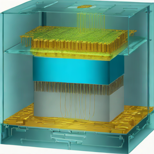
4. HBM: Memory in the Third Dimension
High Bandwidth Memory (HBM) solves the bandwidth problem by going vertical. Instead of placing DRAM chips on a PCB and connecting them through a parallel bus, HBM stacks DRAM dies on top of each other (4, 8, 12, or 16 dies) and connects them with through-silicon vias (TSVs) — vertical holes drilled through the silicon, filled with copper, that carry signals and power between the dies. The stack sits on a silicon interposer next to the processor (GPU or accelerator), connected by a 1,024-bit wide interface running at 3-8 Gbps per pin, for an aggregate bandwidth of 400 GB/s to 1.2 TB/s per stack.
The HBM stack architecture:
    +-------------------+  +-------------------+
    |    DRAM Die 8     |  |    DRAM Die 8     |
    |    (8 Gb)         |  |    (8 Gb)         |
    +--------+----------+  +--------+----------+
             |                      |
    +--------+----------+  +--------+----------+
    |    DRAM Die 4     |  |    DRAM Die 4     |
    +--------+----------+  +--------+----------+
             |    TSVs           |
    +--------+----------+  +--------+----------+
    |    DRAM Die 0     |  |    DRAM Die 0     |
    +--------+----------+  +--------+----------+
             |                      |
    +--------+----------+  +--------+----------+
    |     Logic Die     |  |     Logic Die     |
    |  (PHY + controller)|  |  (PHY + controller)|
    +--------+----------+  +--------+----------+
             |                      |
    +--------+----------------------+----------+
    |          Silicon Interposer              |
    +--------+----------------------+----------+
             |                      |
    +--------+----------+  +--------+----------+
    |    GPU/Accel Die  |  |    GPU/Accel Die  |
    +-------------------+  +-------------------+
Each DRAM die in the stack is a conventional DRAM array, organized into 2-4 channels (called “pseudo-channels” in HBM terminology, to distinguish them from the physical channels in the logic die). Each channel has its own banks, rows, and columns. The logic die at the base of the stack contains the PHY (physical interface) that drives the signals to the interposer, and optionally a built-in self-test (BIST) engine and a temperature sensor.
The key advantage of HBM is bandwidth density. A single HBM3 stack delivers 819 GB/s across a footprint of roughly 100 mm² (including the interposer overhead). A DDR5 DIMM delivers 50 GB/s across a footprint of roughly 3,000 mm² (the PCB area plus the connector). That is a 500× improvement in bandwidth per area. The key disadvantages are cost (HBM stacks are more expensive per gigabyte than DDR5, by a factor of 3-5×) and capacity (an HBM stack is limited to 16-24 GB, while a DDR5 DIMM can hold 512 GB).
5. GDDR: Graphics-Optimized Memory
GDDR (Graphics Double Data Rate) is a variant of DRAM optimized for the high-bandwidth, latency-tolerant workloads of graphics processing. GDDR6 (2018) and GDDR7 (2024) are the current standards. GDDR trades latency for bandwidth: a GDDR6 chip runs at 14-24 Gbps per pin, compared to 4.8-8.8 Gbps for DDR5, but has a CAS latency of 15-20 ns (similar to DDR5 in absolute time, but measured in more clock cycles because the internal clock is faster).
The key architectural differences between GDDR and DDR are:
Point-to-point interface: GDDR uses a point-to-point connection between the memory controller and each DRAM chip, rather than a multi-drop bus. This allows higher signaling rates because there is no stub reflection from multiple DIMMs on the same channel.
Wider internal prefetch: GDDR6 has a 32n prefetch (32 bits of data are read from the array for each external data pin), allowing the internal DRAM arrays to run at a lower frequency while the external interface runs at high speed.
Pseudo-channel mode: Each GDDR6 chip is divided into two pseudo-channels that can operate independently, similar to DDR5’s dual-channel DIMM. This doubles the number of banks and improves random access throughput.
Higher voltage and power: GDDR chips consume more power per gigabyte per second of bandwidth than DDR chips (roughly 7 pJ/bit for GDDR6 vs. 10 pJ/bit for DDR5 — GDDR is actually more efficient per bit, but the absolute power is higher because the bandwidth is higher).
The tradeoff between DDR, HBM, and GDDR can be summarized as:
    +------------+--------+----------+--------+
    |            |  DDR5  |  HBM3    | GDDR7  |
    +------------+--------+----------+--------+
    | BW per chip| 6.4GB/s| 102 GB/s | 48 GB/s|
    | BW per pkg | 50GB/s | 819 GB/s | 576GB/s|
    | Capacity   | 512 GB | 24 GB    | 16 GB  |
    | Latency    | 30 ns  | 50 ns    | 35 ns  |
    | Power/BW   | 10 pJ/b| 3.5 pJ/b | 7 pJ/b |
    | Cost/GB    | $3     | $15      | $8     |
    +------------+--------+----------+--------+
6. The Scaling Wall: Row Hammer and Retention
As DRAM cells shrink, they face two existential threats: row hammer and retention time degradation.
Row hammer is a phenomenon where repeatedly activating (opening and closing) a row of DRAM cells causes charge loss in physically adjacent rows. The mechanism is electromagnetic crosstalk: the rapid voltage swings on the word line couple capacitively to the adjacent word lines, perturbing the floating body of the access transistors and causing them to leak. A malicious program can exploit row hammer to flip bits in rows it does not have permission to access — for example, flipping a page table entry to gain kernel privileges.
Mitigations include:
- Increased refresh rate: Refresh every 32 ms instead of 64 ms. Simple but costs power and performance.
- Target Row Refresh (TRR): The memory controller tracks which rows are being hammered (high activation rate) and refreshes their neighbors. DDR4 and DDR5 include TRR support.
- Error Correction Code (ECC): Single-bit error correction, double-bit error detection (SEC-DED) can correct single-bit flips but not multi-bit flips. DDR5 includes on-die ECC for internal reliability.
Retention time degradation is the gradual decrease in the capacitor’s ability to hold charge as the cell shrinks. At the 10 nm technology node, a DRAM capacitor stores approximately 6 fF and holds roughly 8,000 electrons when charged. The leakage current is on the order of 0.1 fA, meaning the cell loses roughly 1 electron per 10 microseconds. After 64 ms, about 6,400 electrons remain — still enough to detect, but with a shrinking margin. As cells shrink further (below 10 nm), the number of stored electrons drops below 5,000, and the signal margin becomes too small for reliable sensing.
7. Emerging Memory Technologies
The DRAM scaling wall has prompted a search for alternative memory technologies that can scale beyond the 1T1C paradigm. Three leading candidates are:
FeRAM (Ferroelectric RAM). Instead of storing charge on a capacitor, FeRAM stores polarization in a ferroelectric material (typically lead zirconate titanate, PZT, or hafnium oxide, HfO₂). The ferroelectric has two stable polarization states (up and down), which represent logic 0 and 1. The key advantage of FeRAM is non-volatility: the polarization remains even when power is removed. FeRAM also has faster write times (10-50 ns vs. 15-30 ns for DRAM) and lower write energy. The challenges are: (a) the ferroelectric material degrades with cycling (fatigue, typically 10¹⁰-10¹⁴ cycles), and (b) the read is destructive (like DRAM, reading requires sensing the polarization and writing it back).
MRAM (Magnetoresistive RAM). MRAM stores information in the magnetic orientation of a ferromagnetic layer. The basic cell is a magnetic tunnel junction (MTJ): two ferromagnetic layers separated by a thin insulating barrier. The resistance of the junction depends on whether the magnetizations of the two layers are parallel (low resistance, logic 0) or anti-parallel (high resistance, logic 1). Writing is done by passing a current through the junction (spin-transfer torque, STT-MRAM) or by applying a magnetic field (toggle MRAM, mostly obsolete). MRAM is non-volatile, has essentially unlimited endurance (no wear-out mechanism), and can be fast (10-30 ns read/write). The challenges are: (a) the write current is high (100-500 μA per cell), limiting density; (b) the read margin is small (the resistance difference between parallel and anti-parallel states is typically 100-200%), making reliable sensing difficult at advanced nodes.
ReRAM (Resistive RAM). ReRAM, also called memristor memory, stores information as a resistance state in a metal-oxide stack. Applying a voltage pulse changes the resistance by forming or breaking a conductive filament through the oxide. ReRAM offers high density (4F² cell area, compared to 6F² for DRAM, where F is the minimum feature size), fast switching (10-100 ns), and good endurance (10⁶-10¹² cycles depending on the material). The challenges are variability (the filament formation is stochastic, leading to resistance distributions that overlap between states) and the need for a selector device (a transistor or diode in series with each cell to prevent sneak paths through unselected cells).
8. The Memory Hierarchy of Tomorrow
The memory hierarchy of the future will likely be more heterogeneous, not less. DRAM will remain the workhorse for capacity (DDR5 DIMMs, CXL-attached memory pools), HBM will serve bandwidth-hungry accelerators (GPUs, AI engines), and emerging memories will fill specific niches:
- FeRAM for embedded non-volatile memory in microcontrollers (replacing flash and SRAM) and for last-level cache in data center processors (Intel’s 3D XPoint, now discontinued, was a ReRAM variant targeting this space).
- MRAM for radiation-hardened aerospace applications (MRAM is intrinsically immune to single-event upsets) and for cache in automotive processors (where the non-volatility allows instant-on operation).
- ReRAM for compute-in-memory architectures (where the memory element performs computation — vector-matrix multiplication for neural network inference — using Ohm’s law and Kirchhoff’s current law).
The integration of these technologies into the existing memory hierarchy — as a new tier between DRAM and flash, or as a replacement for SRAM caches — is an active area of research and development. The memory wall is not going away, but the tools we have to climb it are becoming more diverse and more capable.
9. Memory Controller Design: The Unsung Hero
The memory controller is the bridge between the processor and the DRAM. It translates read and write requests from the processor’s cache hierarchy into DRAM commands (ACTIVATE, READ, WRITE, PRECHARGE, REFRESH), schedules them to maximize bandwidth while satisfying timing constraints, and manages refresh and error correction.
A modern memory controller is a complex piece of hardware in its own right. It maintains per-bank state (which row is open, when was it last refreshed), a command queue (typically 64-128 entries), and a scheduler that picks the next command based on the current DRAM state and a set of priorities (reads before writes, page hits before page misses, critical requests before non-critical). The scheduler’s decisions have a first-order impact on performance: a well-scheduled controller can achieve 90-95% of the theoretical peak bandwidth, while a poorly scheduled one can drop to 50-60%.
The memory controller also implements the refresh logic. In addition to the mandatory all-bank refresh (every row refreshed every 64 ms), modern controllers support per-bank refresh (each bank can be refreshed independently, allowing other banks to continue serving requests) and adaptive refresh (adjusting the refresh interval based on temperature and row hammer detection).
10. Summary
Memory technology is at an inflection point. The DRAM cell that has served us for five decades is approaching fundamental limits — the capacitor is running out of electrons, the row hammer is getting more aggressive, and the refresh power is becoming a significant fraction of total system power. HBM and GDDR push the bandwidth scaling further, but at the cost of capacity and dollar-per-gigabyte. Emerging memories — FeRAM, MRAM, ReRAM — promise to transcend some of these limits, but each has its own tradeoffs in density, endurance, and manufacturability.
For the systems researcher, memory is the frontier where architecture meets physics. The choices we make about memory technology — DDR vs. HBM, cache vs. scratchpad, volatile vs. non-volatile — ripple through every level of the system stack. Understanding those choices, and the physics that constrains them, is essential to building systems that are not bottlenecked by the slowest component in the hierarchy.
The memory wall has been with us for decades. It will be with us for decades more. But the wall is not featureless — it has handholds, ledges, and the occasional tunnel. HBM, GDDR, and emerging memories are those handholds. The task of the systems architect is to find them, use them, and keep climbing.
11. Memory Interleaving and the Memory Controller Scheduler
The memory controller is the critical piece of hardware that sits between the processor’s last-level cache and the DRAM. Its job is deceptively simple: translate read and write requests into DRAM commands, schedule them for maximum throughput, and manage refresh and error correction. In practice, the memory controller’s scheduler is one of the most performance-critical components in a modern system, and its design is a fascinating case study in real-time resource scheduling under complex timing constraints.
A modern DRAM device has a complex set of timing parameters that the controller must respect. A non-exhaustive list for DDR5 includes: tRCD (RAS-to-CAS delay, ~15 ns), tCL (CAS latency, ~15 ns), tRP (precharge time, ~15 ns), tRAS (minimum row active time, ~40 ns), tRC (row cycle time = tRAS + tRP, ~55 ns), tRRD (row-to-row activation delay, ~5 ns), tFAW (four-activate window, ~30 ns), tRFC (refresh cycle time, ~300 ns for a single bank, up to several microseconds for all-bank refresh), and tREFI (average refresh interval, 7.8 us for DDR5 at 85C). The scheduler must track the state of every bank (which row is open, when was it last activated, when is the next refresh due) and choose commands that maximize data bus utilization while respecting all these constraints.
The scheduling algorithm typically uses a priority-based scheme: (1) High-priority reads that the processor core is waiting on (demand reads) are given highest priority because they directly stall the processor pipeline. (2) Row-buffer hits are prioritized over requests that require a precharge and activate. (3) Writes are batched in a write queue and drained in batches to minimize bus turnaround penalties. (4) Refresh commands have the lowest priority but a hard deadline — every row must be refreshed within 64 ms. The scheduler typically issues refresh commands during idle periods; if the bus is too busy, refreshes preempt reads/writes, causing a brief stall.
The memory controller also handles error correction. DDR5 includes on-die ECC for internal errors, and many server platforms add side-band ECC (SECDED) on the memory channel. The controller must read the ECC bits along with the data, compute the syndrome, and correct single-bit errors transparently.
12. Emerging Memory Standards: CXL, LPDDR, and UCIe
The memory landscape is becoming more diverse, not less. Several emerging standards are reshaping how memory connects to compute:
CXL (Compute Express Link). CXL is a cache-coherent interconnect based on PCIe physical layer. CXL 2.0 supports memory pooling: multiple servers can share a pool of CXL-attached memory, dynamically allocating capacity as needed. CXL 3.0 adds peer-to-peer DMA and fabric capabilities. CXL-attached memory is a fundamentally new tier in the hierarchy: it is slower than local DDR (50-100 ns additional latency) but provides massive capacity (terabytes per server) and flexibility (memory can be allocated between servers on demand). Samsung, SK hynix, and Astera Labs are shipping CXL memory expanders, and Intel’s Sapphire Rapids and AMD’s Genoa server processors include CXL support.
LPDDR (Low-Power DDR). LPDDR5X is the memory standard for mobile devices (smartphones, tablets, laptops). It is optimized for low power (< 5 pJ/bit) rather than high bandwidth, using techniques like dynamic voltage frequency scaling (DVFS), deep power-down modes, and a narrower interface (16 or 32 bits per channel vs. 64 bits for DDR5). LPDDR is beginning to appear in server applications as well: Apple’s M-series processors use LPDDR5 (soldered on-package, not socketed), and Intel’s Lunar Lake laptop platform uses LPDDR5X on-package memory.
UCIe (Universal Chiplet Interconnect Express). UCIe is an open standard for die-to-die interconnect, enabling chiplets from different vendors to communicate over a standard interface. UCIe includes a protocol layer (CXL or PCIe), a link layer, and a physical layer optimized for in-package connections (< 2 mm distance, < 1 pJ/bit energy). UCIe is the key to the chiplet ecosystem: it allows a memory chiplet from Samsung to connect to a compute chiplet from Intel, all within the same package. This disaggregates the memory controller from the DRAM dies, enabling more flexible memory architectures.
13. In-Memory Computing and the Memory-Processor Convergence
The logical conclusion of the memory wall is not just faster memory interfaces, but the elimination of the wall entirely through in-memory computing — performing computation directly within the memory array, so that data never leaves the memory chip. This idea, discussed at length in the Processing-in-Memory post, deserves a brief treatment here as the endpoint of memory technology evolution.
Samsung’s HBM-PIM and SK hynix’s AiM (Accelerator-in-Memory) place 16-wide SIMD units in the logic die of HBM stacks. These units can perform FP16 multiply-accumulate operations at 1-2 TFLOPS per stack, directly on the data stored in the DRAM dies above them. The GPU sends a command (a matrix-vector multiply, a reduction) to the HBM-PIM stack, the PIM units execute it locally, and only the result is returned. This eliminates the interposer bandwidth bottleneck entirely for bandwidth-bound operations like GEMV.
UPMEM’s approach, described in detail in the PIM post, takes this further: each DRAM bank has a small 32-bit RISC core (a DPU) that can execute arbitrary C code on data in that bank. A server with 20 UPMEM DIMMs deploys over 40,000 DPUs, achieving aggregate bandwidth of 6 TB/s for memory-bound, embarrassingly parallel workloads.
The long-term trajectory is clear: memory and compute are converging. Whether through HBM-PIM (domain-specific accelerators in the memory stack), UPMEM (general-purpose cores in DRAM), or future architectures (ReRAM-based compute-in-memory for neural network inference), the trend is toward computation happening where the data lives, not where the CPU sits. This convergence will reshape the memory hierarchy as profoundly as the introduction of caches reshaped it in the 1970s.
14. Summary (Extended)
The future of memory technology is not a single winner but a diverse ecosystem of technologies, each optimized for a different point in the capacity-bandwidth-latency-cost space. DDR will remain the workhorse for capacity. HBM will serve bandwidth-hungry accelerators. GDDR will power graphics and gaming. CXL will enable memory pooling and composability. Emerging memories (FeRAM, MRAM, ReRAM) will fill niches — embedded NVM, compute-in-memory, radiation-hardened applications. And in-memory computing will blur the line between memory and processor, turning the memory hierarchy from a passive storage system into an active compute fabric.
15. Memory Reliability, Fault Tolerance, and the Scale-Out Challenge
As memory capacities grow — terabyte-scale servers, petabyte-scale clusters — the probability of a memory error becomes non-negligible. A single DRAM device with a soft error rate (SER) of 10^-12 errors per bit per hour, with 64 Gb of capacity, experiences roughly one soft error per 1,500 hours (about 2 months). A server with 2 TB of DRAM (32 × 64 Gb devices) experiences roughly one soft error every 50 hours. A cluster with 1,000 such servers experiences about 20 soft errors per hour.
These soft errors — caused by cosmic rays, alpha particles from packaging materials, or thermal neutrons — are not hypothetical. Google’s 2009 study of DRAM errors in its fleet found that 8% of DIMMs experienced at least one correctable error per year, and that error rates increased with temperature and utilization. The study also found that correctable errors were a strong predictor of uncorrectable errors (a DIMM that experienced many correctable errors was likely to experience an uncorrectable error soon).
Memory reliability, once a niche concern for aerospace and high-assurance systems, is now a mainstream concern for cloud operators. The response has been a combination of hardware and software techniques:
Chipkill and Advanced ECC. Standard SECDED (single error correction, double error detection) can correct a single-bit error and detect a double-bit error, but cannot correct multi-bit errors caused by a single event upset affecting multiple adjacent cells. Chipkill ECC (used in many server platforms) can correct multi-bit errors confined to a single DRAM chip by striping ECC across multiple chips. Advanced ECC schemes (like AMD’s “Advanced Memory Protection”) use symbol-based codes to correct errors spanning multiple bits.
Memory scrubbing. A background process reads every memory location periodically (typically every 24 hours), checks the ECC, and corrects any single-bit errors before they accumulate into multi-bit errors. Scrubbing reduces the probability of an uncorrectable error by proactively correcting latent errors.
Page retirement and DIMM sparing. When a memory page experiences repeated correctable errors, the operating system can retire that page (mark it as unusable and map it out of the virtual address space). When a DIMM experiences excessive errors, the memory controller can activate a spare DIMM (if available) and copy the data from the failing DIMM to the spare, then take the failing DIMM offline. These techniques provide graceful degradation in the face of hardware faults.
Software-level resilience. Applications can be designed to tolerate memory errors through replication (storing critical data in two memory locations and comparing on read), checksums (storing a CRC alongside each data structure and validating on access), or erasure coding (splitting data across multiple servers with redundancy, so that the failure of any single server does not cause data loss).
16. Conclusion: The Memory Wall is a Design Constraint, Not a Dead End
The memory wall — the exponentially growing gap between processor speed and memory bandwidth — has been the defining constraint of computer architecture for two decades. It has not gone away. But the tools for managing it have become more sophisticated: HBM for bandwidth-hungry accelerators, CXL for flexible memory pooling, GDDR for graphics, emerging memories for niche applications, and in-memory computing for eliminating the wall entirely. The memory hierarchy of 2035 will look very different from that of 2025 — more heterogeneous, more distributed, more intelligent — but the fundamental goal remains: getting data to the compute units that need it, as quickly and efficiently as possible, within the bounds set by physics and economics.
Memory technology is the substrate on which all computing rests. As we push the limits of DRAM scaling and explore new memory technologies, we are not just solving technical problems — we are reshaping the foundation of every computer system, from the smallest IoT sensor to the largest exascale supercomputer. The future of memory is diverse, intelligent, and deeply integrated with compute in ways that were unimaginable when the first DRAM cell was demonstrated in 1966.